


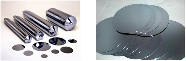
The Raw Silicon Wafer
Specifications: 3 inch to 4 inch monocrystalline silicon N light silicon chip, 3 inch to 4 inch silicon N/P type silicon wafer
By adding phosphorus or boron doped, using MCZ technology, the production size is 3 inch, 4 inch, 0.003-55 resistor.Cm, 200-350um thickness of different type N or type P monocrystalline silicon wafer, and silicon wafer edge positioning production according to customer requirements, chamfered silicon, N silicon, P silicon etc. the resistivity and thickness, production according to customer requirements.
- File name
- File download
- The Raw Silicon Wafer parameter configuration table
-
- 3-inch mono crystal silicon N-type light doped waferparameter configuration table
-
- 4-inch mono crystal silicon N-type light doped wafer parameter configuration table
-
- 3-inch mono crystal silicon heavy doped wafer parameter configuration table
-
- 4 inch monocrystal silicon heavy doped wafer parameter configuration table
-
3-inch mono crystal silicon N-type light doped wafer
|
ResistivityΩ·CM |
Thicknessμm |
Crystal Orientation |
Lifeμs |
External Diametermm |
Dopant |
Form |
Radial uniformitty of resistivity |
||||
|
AS cut |
Lapping |
Chamfering |
Flattingiece |
||||||||
|
5-10 |
200-350 |
<111> |
>100 |
76.2±0.3 |
Phosphorus |
√ |
√ |
√ |
√ |
≤20% |
|
|
10-15 |
200-350 |
<111> |
>100 |
76.2±0.3 |
Phosphorus |
√ |
√ |
√ |
√ |
≤20% |
|
|
15-20 |
200-350 |
<111> |
>100 |
76.2±0.3 |
Phosphorus |
√ |
√ |
√ |
√ |
≤20% |
|
|
20-25 |
200-350 |
<111> |
>100 |
76.2±0.3 |
Phosphorus |
√ |
√ |
√ |
√ |
≤20% |
|
|
25-30 |
200-350 |
<111> |
>100 |
76.2±0.3 |
Phosphorus |
√ |
√ |
√ |
√ |
≤20% |
|
|
30-35 |
200-350 |
<111> |
>100 |
76.2±0.3 |
Phosphorus |
√ |
√ |
√ |
√ |
≤20% |
|
|
35-40 |
200-350 |
<111> |
>100 |
76.2±0.3 |
Phosphorus |
√ |
√ |
√ |
√ |
≤20% |
|
|
40-45 |
200-350 |
<111> |
>100 |
76.2±0.3 |
Phosphorus |
√ |
√ |
√ |
√ |
≤20% |
|
|
45-50 |
200-350 |
<111> |
>100 |
76.2±0.3 |
Phosphorus |
√ |
√ |
√ |
√ |
≤20% |
|
|
50-55 |
200-350 |
<111> |
>100 |
76.2±0.3 |
Phosphorus |
√ |
√ |
√ |
√ |
≤20% |
|
4-inch mono crystal silicon N-type light doped wafer
|
ResistivityΩ·CM |
Thicknessμm |
Crystal Orientation |
Lifeμs |
External Diametermm |
Dopant |
Form |
Radial uniformitty of resistivity |
||||
|
AS cut |
Lapping |
Chamfering |
Flattingiece |
||||||||
|
5-10 |
200-350 |
<111> |
>100 |
101.6±0.3 |
Phosphorus |
√ |
√ |
√ |
√ |
≤20% |
|
|
10-15 |
200-350 |
<111> |
>100 |
101.6±0.3 |
Phosphorus |
√ |
√ |
√ |
√ |
≤20% |
|
|
15-20 |
200-350 |
<111> |
>100 |
101.6±0.3 |
Phosphorus |
√ |
√ |
√ |
√ |
≤20% |
|
|
20-25 |
200-350 |
<111> |
>100 |
101.6±0.3 |
Phosphorus |
√ |
√ |
√ |
√ |
≤20% |
|
|
25-30 |
200-350 |
<111> |
>100 |
101.6±0.3 |
Phosphorus |
√ |
√ |
√ |
√ |
≤20% |
|
|
30-35 |
200-350 |
<111> |
>100 |
101.6±0.3 |
Phosphorus |
√ |
√ |
√ |
√ |
≤20% |
|
|
35-40 |
200-350 |
<111> |
>100 |
101.6±0.3 |
Phosphorus |
√ |
√ |
√ |
√ |
≤20% |
|
|
40-45 |
200-350 |
<111> |
>100 |
101.6±0.3 |
Phosphorus |
√ |
√ |
√ |
√ |
≤20% |
|
|
45-50 |
200-350 |
<111> |
>100 |
101.6±0.3 |
Phosphorus |
√ |
√ |
√ |
√ |
≤20% |
|
|
50-55 |
200-350 |
<111> |
>100 |
101.6±0.3 |
Phosphorus |
√ |
√ |
√ |
√ |
≤20% |
|
3-inch mono crystal silicon heavy doped wafer
|
ResistivityΩ·CM |
Thicknessμm |
Crystal Orientation |
Model |
External Diametermm |
Dopant |
Form |
Radial uniformitty of resistivity |
||||
|
AS cut |
Lapping |
Chamfering |
Flattingiece |
||||||||
|
0.003-0.005 |
200-350 |
<111> |
N/P |
76.2±0.3 |
Phosphorus/Boron |
/ |
√ |
√ |
√ |
/ |
|
|
0.005-0.008 |
200-350 |
<111> |
N/P |
76.2±0.3 |
Phosphorus/Boron |
/ |
√ |
√ |
√ |
/ |
|
|
0.02-0.03 |
200-350 |
<111> |
N/P |
76.2±0.3 |
Phosphorus/Boron |
/ |
√ |
√ |
√ |
/ |
|
4 inch monocrystal silicon heavy doped wafer
|
ResistivityΩ·CM |
Thicknessμm |
Crystal Orientation |
Model |
External Diametermm |
Dopant |
Form |
Radial uniformitty of resistivity |
||||
|
AS cut |
Lapping |
Chamfering |
Flattingiece |
||||||||
|
0.003-0.005 |
200-350 |
<111> |
N/P |
101.6±0.3 |
Phosphorus/Boron |
/ |
√ |
√ |
√ |
/ |
|
|
0.005-0.008 |
200-350 |
<111> |
N/P |
101.6±0.3 |
Phosphorus/Boron |
/ |
√ |
√ |
√ |
/ |
|
|
0.02-0.03 |
200-350 |
<111> |
N/P |
101.6±0.3 |
Phosphorus/Boron |
/ |
√ |
√ |
√ |
/ |
|